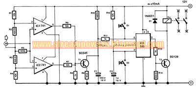
Audio Controlled Mains Switch Circuit diagram. It is often useful for audio or video equipment to be switched off automatically after there has been no input signal for a while. The function of the on-off switch in such equipment is then taken over by switch S2 in the accompanying diagram. It remains, however, possible to switch off manually by means of Si. Automatic switch-off occurs after there has been no input signal for about 2 minutes: this delay makes it possible for a new record or cassette to be placed in the relevant machine.
The audio input to the proposed circuit may be taken from the output of the relevant TV set, amplifier, or whatever. The input earth is held at + 6 V with respect to the circuit earth by potential divider Ri-R2-R3-R4. The two 741s function as comparators: the output of ICi goes high when the in- put signal is greater than + 50 mV, whereas the out- put of IC2 goes high when the input signal becomes more negative than -50 mV. Resistors R6, R7, and R8 form an OR gate that drives transistor Ti. If the output of either ICi or IC2 is logic 1, Ti conducts.
Audio Controlled Mains Switch Circuit diagram :


Audio Controlled Mains Switch Circuit Diagram
The 555 operates as a retrigger able monostable, whose period is determined by Rio and Ci. The device is triggered when its pin 2 is earthed by the closing of S2. Its output, pin 3, then remains high for 1 to 2 minutes, depending on the leakage cur- rent of the 555.
The monostable resets itself as soon as the potential across Ci exceeds a certain value. As long as there is an input signal to the circuit, Ti conducts and Ci remains uncharged. As soon as the audio signal ceases, Ti switches off, and Ci charges until the potential across it is sufficient to reset the 555. The monostable may also be reset by closing Si, which connects pin 6 of the 555 to + 12 V.

When IC3 is reset, Ci is discharged via its pin 7. Resistor Rrn serves as protection, because without it Ti could short-circuit the supply lines. When the output of IC3 goes high, T2 conducts, the relay is energized, and the relay contacts switch on the mains voltage as appropriate. To counter the induced potential when the relay contacts close, which could damage T2, diode Di has been connected in parallel with the relay coil.
Comments
Post a Comment