Basically the circuit designed above have a very simple way of working, where the circuit is designed so that does not happen short circuit or short circuit between the voltage supply with batteries that will be in-charge.
It is true that if any one wants to try to direct mengghubungkan between supply with batteries then the batteries can be sure will be filled. But the current flowing through a charged battery can not be controlled and if the battery is full, the batteries will be damaged or worn out if it remains on the short circuit condition.
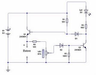
Working Principle Battery Charger
By the time we put an empty battery charging terminals, transistor Q1 will be activated immediately because the current flows through R1 and would trigger a transistor Q1 base. In this condition the flow that would fill the batteries mostly comes from the collector of Q1 is connected directly to the positive terminal of supply. Then during the charging process increases the battery voltage will increase the current flowing in Q2 base via 10 Kohm R5, VR1 and diode D2. VR1 is a component that is used as an initial calibration to determine the exact position in the planning process of switching circuit. For VR1 you can use a trimpot or potensio according to your taste. At the beginning of filling, arrange potensio at position D3 LED indicators on the condition of death, and the current flowing into the collector of Q1 is not too big and not too small.
If the battery is fully charged, the LED indicator will light up automatically because of an increase in voltage on the battery charge will cause the increase of current flowing at the base of transistor Q2 and will terminate the charging cycle due to transistor Q1 having a cut-off due to lack of base current. Why on condition Q1 base current will experience a shortage of this is because almost all the current flowing in R1 10 Kohm will switch to a diode D1 which is logically connected directly with ground experience due Q2 saturated.
.
Component List
1. Resistors: R1 (10 Kohm), R2 (680 ohms), R3 (100 Kohm), R5 (10 Kohm) and VR1 (Potensio / trimpot = 100 Kohm)
2. Diodes: D1 & D2 (IN4002) and D3 (Led)
3. Transistors: Q1 and Q2 (2N3904)
4. 9 volt power supply
Comments
Post a Comment